I was fortunate to get to familiarise myself with our research group’s state-of-the-art Kelvin probe for a graduate research project I was part of. On a very broad level, The Kelvin probe (KP) is a method that allows the experimenter to correlate the Fermi level of the sample to the absolute reference electrode scale, which is a useful thing for solar cells and many other kinds of materials.
In this blog post, which is a distillate of a longer note I wrote in my electronic labnotebook a while ago, I will give a short introduction to KP from a beginning experimenter’s perspective. Note that this post is limited to Kelvin probe microscopy, and does not discuss Kelvin probe force microscopy (except perhaps in passing).
At the end of this post we have collected some links to other KP resources on the web.
History of the Kelvin probe technique
The Kelvin probe method was first demonstrated in 1898 by Lord Kelvin [1]. The two plates forming a capacitor were repeatedly moved by hand. Kelvin and his contemporaries used the instrument mainly to study the “contact electrification” of metals.
The next major improvement was in 1928 when Zisman developed a way to automatically vibrate one of the metal plates (“for hours”) by way of an air blast pointed at a piano wire [2]. The work was part of Zisman’s masters thesis at MIT, and published a few years later.
I think the study of the operation of the forebears of scientific instruments can be very helpful in understanding their modern counterparts. So, here I will devote a few lines to go through the operation of an early version of the Kelvin probe (mainly based on Zeisman’s paper).

Figure 1: Electric circuit diagram I made of a manually operated Kelvin probe based on a sketch in [2]. The “tip” (labelled A) and the specimen (B) form a capacitor. The capacitor is connected to a potentiometer (a variable resistor and battery) via switch S2, and to an electrometer via switch S1. This diagram represents the most common way of measuring the contact potential difference (CPD) before the introduction of Zisman’s vibrating plate. We can use this diagram to better understand the operation of a modern Kelvin probe.
The experimenter can monitor the charge on A using the electrometer (given that S1 is closed, of course). If electrode A is moved away from B (i.e., increasing the distance), the capacity of the capacitor AB will decrease and an electric charge will be transferred to the electrometer causing its readout to change.
Now let’s assume that we keep S1 open, but close S2 and set the potentiometer so that the CPD is precisely counter-acted. We would then have neutralised the charge between A and B, and if we now open S2 and close S1 again, the electrometer should no longer display a changing readout when we move the two plates away from each other.
So by gradually increasing the distance between A and B, while determining the CPD and electrometer readout for each distance (an admittedly laborious process), we could note at which applied potential difference the charge displays a minimum (ideally it becomes zero) and that’s our CPD. Of course, happening to distance the plates precisely at the zero-charge point is quite unlikely, so a slightly better method is to plot the electrometer readout against the applied potential difference – the intercept on the axis along which we plot the potential difference will then be the CPD.
The major achievement of Zisman’s vibrating setup was that it made away with the whole process of moving the plates by hand, by exploiting the fact that periodically (and uniformly) vibrating capacitor plates will give rise to a steady AC current whose amplitude will depend on the capacitance (i.e., charge) on said capacitor, with both the capacity and the AC current being zero at the point where the applied potential difference balances the CPD.
Zisman’s setup also replaced the electrometer readout with speakers, that emitted a sound until the applied potential difference balanced the CPD, at which point they went silent. This way a measurement merely consisted of balancing the resistance on the potentiometer until no sound was heard, which could be accomplished by the experimenter in a matter of seconds.
The contact potential difference (CPD)
The existence of a contact potential difference between two dissimilar metals was discovered by Volta in 1801 (“Volta’s electromotive force of contact”, according to [1]), you will therefore sometimes find authors preferring to call it the Volta potential difference.
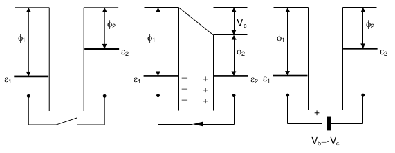
Figure 2: Left: two different metals in proximity, no electrical circuit between them. Center: now with an external electrical circuit connecting them. The two surfaces become equally and oppositely charged. Right: introducing a variable electromotive force (EMF) in the external circuit allows us to nullify the electric field, effectively measuring it. Image reproduced from a KP Technology manual.
The left panel of figure 2 shows two different metals in close proximity, but isolated (without electrical contact between them). Dissimilar metals will have different work functions (\(\phi_1\), \(\phi_2\)) and their Fermi levels are thus not aligned (\(\varepsilon_1\), \(\varepsilon_2\)). This system acts like a parallel plate capacitor, where the capacitance is equal to the ratio of the amount of charge to the potential difference,
\[\begin{equation} C = \frac{Q}{\Delta V} \end{equation}\]
and the capacitance is also inversely proportional to the distance between the two surfaces
\[\begin{equation} C = \varepsilon_\text{r}\varepsilon_\text{0}\frac{A}{d} \end{equation}\]
In the center panel of figure 2 the metals are now connected via an external circuit, causing electrons to flow from the metal with the smaller work function to that with the larger work function. This causes the smaller work function metal to charge positively and the larger work function metal to charge negatively. This charge-separation across the metal-metal interface is driven by the work function difference, and the charge-separation buildup stops once the created electric field (due to the charge-separation) compensates for the work function difference. At this equilibrated state, the Fermi levels of both metals are equal (\(\varepsilon_1 = \varepsilon_2\)), and the so-called contact potential, \(V_\text{c}\), between the electrodes exactly equals the work function difference.
The right panel of figure 2 shows that by introducing a variable EMF in the external circuit, we can find the potential at which the contact potential is nulled (i.e., where \(V_\text{b} = -V_\text{c}\)). This is called the backing potential (or sometimes the counter potential) and forms the basis for the operation of a Kelvin probe.
The work function
As we have already seen, Lord Kelvin demonstrated that a potential is generated between two conductors when they are brought into contact (electrons in the material with the lower work function flow to the one with the higher work function). This contact potential difference (CPD) depends on the work function of the two materials in contact:
\[\begin{equation} V_\text{CPD} = \frac{\phi_\text{tip} - \phi_\text{sample}}{e} = \frac{\Delta\phi}{e} \end{equation}\]
where \(\phi_\text{tip}\) is the work function of the tip of the Kelvin probe, and \(\phi_\text{sample}\) is the work function of the sample.
So, what is the work function? In short, the work function is the amount of energy needed to release electrons from the material. More stringently, the work function is defined as the minimum work that is required to extract an electron from within the sample to a position just outside the sample (carrying zero kinetic energy).
“Just outside the sample” is far enough from the sample surface that the electron is outside the surface dipole layer (which translates to a few nanometers). For an uncharged sample the energy of “just outside the sample” and very far from it (i.e., “at infinity”) are the same, and equivalent to the vacuum level, \(E_\text{VAC}\). Note that there is a possible source of confusion here, as some authors denote the “just outside the sample” position as the “vacuum level” and the “at infinity” position as the “vacuum level at infinity” (this latter being the vacuum level intended when comparing against other reference electrodes). In the following, I intend to call the position “just outside the sample” for just that, and the “at infinity” position for the “vacuum level”, i.e., \(E_\text{VAC}\) (please correct me if you discover any inconsistencies!). As we have noted, for an uncharged sample there is effectively no difference in energy between these positions. But most samples will be charge (here charged does not mean that the whole material carries an effective charge, which is a physical impossibility) but rather that the surface in contact with the probe is charged, which is the case for many semiconductors, e.g., crystals with a non-centrosymmetric symmetry will have one direction that is more polar than the others (cf. piezoelectric crystals). Anyway, the point is that for most real-world materials, the point at which the vacuum level is defined actually matters.
The work function for an uncharged sample is comprised of the chemical work and the electrostatic work necessary for transporting the charged electron through the dipole layer at the surface: [3]
\[\begin{equation} \phi = -\mu_\text{e} + e\chi = -(\mu_\text{e} - e\chi) \end{equation}\]
where \(\mu_\text{e}\) is the chemical potential (i.e., the chemical work to transfer the electron from infinity into the sample, hence the minus sign), \(e\) is the electron charge, and \(\chi\) is the so-called dipole or surface potential (this is the potential drop between just inside the sample to just outside of it). Note that I have chosen to use lower-case phi (\(\phi\)) to symbolise the work function rather than upper-case Phi (\(\Phi\)).
If the sample is charged an additional work component is necessary to transfer the electron to a position infinity far away, namely \(e\psi\), where \(\psi\) is the Volta potential and is due to surface charges [3].
In a semiconductor, the work function can be expressed as a function of the position of \(E_\text{VAC}\) and the Fermi level of the material, \(E_\text{F}\), of which the latter in turn depends on the material’s density of states, temperature, carrier density and doping concentration: [4]
\[\begin{equation} \phi = E_\text{VAC} - E_\text{F} \end{equation}\]
[The work function, \(\psi\),] is measured as the combination of the two components, which cannot be experimentally separated. The dominant one, i.e., the bulk component, corresponds to the chemical potential that derives from the electronic density and density of states in the solid. Its calculation involves the determination of the difference in energy between the \(N\) and \(N-1\) electron system. The surface component, also known as surface dipole component, corresponds to an additional potential step (positive or negative) that originates with a redistribution of charges at the surface of the solid. This component is inherent to the surface of the solid and exists only at the solid–vacuum interface. — [4]
The surface of the solid thus represents an energy barrier that the electron at the Fermi level must overcome to reach the vacuum level (free space). This also means that \(\phi\) and \(E_\text{VAC}\) are meaningful only in relation to the surface of the solid material.
The redistribution of charges at the surface of a material, which gives rise to the surface dipole, takes on several possible mechanisms. The generic mechanism for metal surfaces is the “spill out” of electrons into vacuum. Deep in the metal, the electron density along the \(z\) direction perpendicular to the surface is constant (at least in a simple jellium-type model), but as the lattice abruptly terminates at the surface, electrons tunnel out of the solid over some small distance (Ångströms), creating a negative sheet of charges outside the solid and leaving a positive sheet of uncompensated metal ions in the surface and sub-surface atomic planes. This double sheet of charges creates a potential step that increases the electron potential just outside the surface, effectively raising \(E_\text{VAC}\) and [\(\psi\)]. This electronic redistribution and potential step depends sensitively on the atomic arrangement at the surface of the solid […] — [4]
This makes Kelvin probe microscopy an exceptionally sensitive indicator of surface conditions and affected by absorbed or evaporated layers, surface charging, oxide layer imperfections, surface contamination, and more.
Principle of operation of a Kelvin probe
It appears to me that most contemporary Kelvin probe’s use the so-called Baikie system (so named after its inventor, professor Iain Baikie, the founder of KP Technology), where the CPD is determined using what is called an “off-null height-regulated” method where the signal generated by the vibrating electrode is measured far from the electric balance point, meaning the generated current amplitude depends linearly on the backing potential, and thus the point where the current amplitude is equal to zero determines the CPD [5]. This significantly reduces noise compared to the traditional method of determining CPD.
The Kelvin probe can be considered a natural reference electrode, and the only absolute reference electrode available to us. Still, to obtain the work function of a sample versus the absolute vacuum level the probe must first be calibrated against a reference material with a known work function.
When the probe is vibrated, a varying capacitance is produced: \[\begin{equation} C_\mathrm{K}(t) = \varepsilon_\mathrm{r} \varepsilon_\mathrm{0} \frac{A}{d(t)} \end{equation}\] where \(C_\mathrm{K}(t)\) is the time-varying Kelvin capacitance, \(\varepsilon_\mathrm{0}\) is the permittivity of free space, \(\varepsilon_\mathrm{r}\) is the relative permittivity, \(A\) is the surface area of the capacitor plate and \(d(t)\) is the time-dependent separation between the capacitor plates.
Assuming the tip–sample separation can be represented by a periodic sinusoidal displacement \(d(t) = d_\mathrm{0} + d_\mathrm{1}\sin(\omega t)\), then the varying capacitance becomes \[\begin{equation} C_\mathrm{K}(t) = \frac{C_\mathrm{0}}{1 + \frac{d_\mathrm{1}}{d_\mathrm{0}} \sin(\omega t)} \end{equation}\] where \(C_\mathrm{0}\) is the mean capacity, \(\omega\) is the angular frequency of vibrations in radians per seconds, \(d_\mathrm{0}\) is the mean distance between tip and probe, and \(d_\mathrm{1}\) is the amplitude of tip motion (the ratio \(d_\mathrm{1}/d_\mathrm{0}\) is the so-called modulation index). I am going to skip how this ties into the electronic circuit design of the Kelvin probe, and directly proceed to tell you that the instantaneous total surface charge on the tip of the probe evaluates to: \[\begin{equation} Q_\mathrm{S} = C_\mathrm{K} (V_\mathrm{b} + V_\mathrm{c}) \end{equation}\] I am going to skip some more steps in this derivation, and straight away note that this leads to the output signal produced by the Kelvin probe using the “off-null height-regulated” method, namely the peak-to-peak voltage \(V_\mathrm{ptp}\). This is then plotted against the backing potential and the intercept of the resultant straight line on the ordinate is the point where \(V_\text{b} + V_\text{c} = 0\). Et voilà, we have our CPD, and assuming we can determine or know the work function of the probe tip (the other half of the capacitor), calculating the work function of our sample is only a subtraction away.
When discussing the determination of absolute work function of materials we would be amiss to not mention another method that can do the job, namely photoemission spectroscopy (PES). The main advantage of KP over PES with regards to semiconductor materials is that KP can be performed in the dark, which gives the experimenter a way to avoid the confounding effect of band bending that may occur under illumination [4]. Another advantage is that KP can be done in air, whereas PES requires vacuum (this may or may not be considered an advantage, depending on your vantage point). Work function measurements made in air are affected by the adsorption of atmospheric gasses, such as oxygen [5], which is why modern KP chambers allow purging with nitrogen and humidity control.
If you have read this far you might be interested in the simple
R package kptech
I wrote which helps you import and plot data from a KPTech Kelvin probe.
Kelvin probe force microscopy (KPFM)
Kelvin probe force microscopy was first proposed by [6], and allows the experimenter to obtain both topographic and potential images of the sample’s surface. It is based on atomic force microscopy (AFM).
The CPD is determined as in a regular KP, and the cantilever deflection (due to electrostatic repulsion, it is not touching the sample’s surface) is normally detected by a photodetector.
Notes and links
- Tutorial on Kelvin probe measurements, Rudy Schlaf (University South Florida)
- Translation guide for discussing electron energy concepts, Steve Byrnes (University of California, Berkeley)
- KP Technology
There’s a bunch of questions on StackExchange related to the work function:
- Fermi energy, Fermi level and work function
- Definition of Fermi energy and Fermi level
- Why is Fermi energy not at the top of valence band?
- Work function and ionisation energy are different
- Work function definition: vacuum, image forces (and a comparison with PES)
- An explanation of vacuum level and Fermi level for metals and semiconductors in terms of Schottky-Mott theory
- A question and answer on terminology, cf. Byrnes’ translation guide
- Surface potential and work function
- The photoelectric effect and work function
- Local work function vs work function
- On calculating the work function of metals
- Finding the work function by measuring the kinetic energy of the ejected electron (i.e, PES again)
- Work function with two materials in contact
- Making clear the difference between ionisation potentials (atoms) and work function (bulk)
- Metal-oxide semiconductor in contact with metal: band bending
Youtube gives a few hits for “kelvin probe”:
- Apparently surface potential of bacteria can be measured using Kelvin probe force microscopy, Journal of Visualized Experiments.
- Product demo of a scanning Kelvin probe by BioLogic.
- A recorded seminar on Kelvin probe force microscopy of field-effect transistors by Dr Mukherjee, Israel Institute of Technology.
- A tutorial on fundamental theory and application of KPFM.
- An animation of the operation of the probe in Kelvin probe force microscopy.
- An animated presentation on Kelvin probe force microscopy from a course on Nanoscale imaging at Rice University.
- A demonstration of a Kelvin probe at the Instytut Fotonowy in Cracow.